Paraflasher: Difference between revisions
Linux junkie (talk | contribs) No edit summary |
Linux junkie (talk | contribs) |
||
| Line 178: | Line 178: | ||
===Data Circuit=== | ===Data Circuit=== | ||
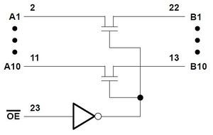
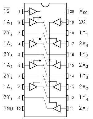
The LPCflasher is connected to the PC’s Parallel port via a DB25 Parallel extension cable and is run in SPP mode. | The LPCflasher is connected to the PC’s Parallel port via a DB25 Parallel extension cable and is run in SPP mode. The 10-Bit FET Bus Switch With Level Shifting is connected to data lines D0 – D6 convert the data signals from 5V to 3.3V needed by the flash chip. The parallel port data lines D0, D1, and D2 are used for driving the control signals LCLK, LFRAME, and RST. The parallel port data lines D3, D4, D5, and D6 are used for bi-directional data transfers of the corresponding LAD0, LAD1, LAD2, and LAD3 lines. LAD0, LAD1, LAD2, and LAD3 lines are also buffered and feed back to the parallel port /Error, /SELIN, /PE, and /Ack signals. The 74HC244 is an advanced high-speed CMOS Octal Bus Buffer that acts as a simple signal buffer between D0, D1, /Error, /SELIN, /PE, /Ack and the LCLK, LFRAME, LAD0, LAD1, LAD2, LAD3 lines. | ||
[[Image:SN74CBTD3861.jpg|right|thumb|SN74CBTD3861]] | |||
[[Image:M74HC244B1R.jpg|right|thumb|M74HC244B1R]] | [[Image:M74HC244B1R.jpg|right|thumb|M74HC244B1R]] | ||
| Line 247: | Line 247: | ||
|} | |} | ||
===Power Circuit=== | ===Power Circuit=== | ||
I did not like the original power circuit design of using a wall-wart type power supply and a LED as voltage regulator, so I came up with the following and it works pretty slick. The LPCflasher is powered by USB via a USB printer cable. The jack is a USB type B. All of the grounds from every component requiring a ground is connected together. The +5 VDC from USB is connected to a PTC Resettable Fuse with trip current of 0.5 Amp (500ma). USB v2.0 specifies a maximum of 500mA so this will protect the PC’s USB port from any damage caused by short circuits, etc. If the PTC Resettable Fuse is tripped, disconnect the power source (USB) and wait a few seconds for the PTC Resettable Fuse to cool down and reset. Next I put in a simple LED circuit just for user aesthetics, so you know your getting power from USB. If you want to use a different color LED or if the blue LED is too bright you can adjust the ohms of the resistor. A 5V power line branches off from here and continues to the header to power a 5V flash chip. I went with the LM1084IT-3.3 voltage regulator because it is designed to convert 5V to a fixed output of 3.3V to power the octal buffer and a 3.3V flash chip. Simple and effective. National Semiconductor recommends for a 5V to 3.3v conversion to place a 10 UF Tantalum capacitor on both the input and output lines of the voltage regulator. They recommend using Tantalum capacitors for stability because their equivalent series resistance (ESR) is lowest at any temperature. The 3.3V line powers the 74HC244 octal buffer and continues on to the header to power a 3.3V flash chip. | I did not like the original power circuit design of using a wall-wart type power supply and a LED as voltage regulator, so I came up with the following and it works pretty slick. The LPCflasher is powered by USB via a USB printer cable. The jack is a USB type B. All of the grounds from every component requiring a ground is connected together. The +5 VDC from USB is connected to a PTC Resettable Fuse with trip current of 0.5 Amp (500ma). USB v2.0 specifies a maximum of 500mA so this will protect the PC’s USB port from any damage caused by short circuits, etc. If the PTC Resettable Fuse is tripped, disconnect the power source (USB) and wait a few seconds for the PTC Resettable Fuse to cool down and reset. Next I put in a simple LED circuit just for user aesthetics, so you know your getting power from USB. If you want to use a different color LED or if the blue LED is too bright you can adjust the ohms of the resistor. A 5V power line branches off from here and continues to the header to power a 5V flash chip. I went with the LM1084IT-3.3 voltage regulator because it is designed to convert 5V to a fixed output of 3.3V to power the octal buffer and a 3.3V flash chip. Simple and effective. National Semiconductor recommends for a 5V to 3.3v conversion to place a 10 UF Tantalum capacitor on both the input and output lines of the voltage regulator. They recommend using Tantalum capacitors for stability because their equivalent series resistance (ESR) is lowest at any temperature. The 3.3V line powers the 74HC244 octal buffer and continues on to the header to power a 3.3V flash chip. | ||
Revision as of 02:58, 28 November 2008
THIS PAGE IS STILL UNDER CONSTRUCTION AND IS NOT LINKED ANYWHERE YET
Welcome to The LPCflasher Project. Open source hardware for developing open source software.
The project is maintained by Joseph Smith.
Overview
The LPCflasher is low-cost simple flash programming device. It can be used to flash a variety of LPC flash chips and firmware hubs (FWH). The hope is someday it will also be able to support SPI chips. It is also meant to be modular so you can flash a variety flash chip packages. The LPCflasher is based on an old LPC programmer built to flash LPC chips on the xbox, the LPC^2 (Low Parts Count LPC Programming Cable). The LPCflasher is not for sale, it is meant for that "do-it-yourself" kind of person. Although if the project becomes popular, bare PCB's could be produced and sold at cost. Anyone with novice to moderate soldering skills can build one.
Other Pictures
-
Top
-
Ugly Bottom
-
Front
-
Right
-
Rear
-
Left
Components
| Component | Recomended Specs | Part Used | Price Paid ($US) |
|---|---|---|---|
| DB25 Connector |
|
ITW McMurdo DB25PNF | 3.82 |
| 10-Bit FET Bus Switch With Level Shifting |
|
Texas Instruments SN74CBTD3861DW | 0.64 |
| SOIC To DIP Adapter |
|
MIND_TEK SOIC surface mount PCB adaptor | 1.60 |
| Octal Buffer |
|
STMicroelectronics M74HC244B1R | 0.40 |
| Header Connector |
|
Molex 10897162 | 1.19 |
| USB B Connector |
|
Adam Technologies USB-B-S-RA | 0.39 |
| PTC Resettable Fuse |
|
Littelfuse 60R025XU | 0.26 |
| Blue LED |
|
OPTEK Technology OVLFB3C7 | 0.74 |
| LED Resistor |
|
Vishay/Dale CPF2200R00FKE14 | 0.42 |
| Linear Voltage Regulator |
|
National Semiconductor LM1084IT-3.3/NOPB | 2.83 |
| 2 Tantalum Capacitors |
|
Vishay/Sprague 173D106X9010VE3 | 0.56 X 2 |
| Breadboard PCB |
|
A piece of Roth Electronik 26M2198 | Already had (5.93) |
| Hook-Up Wire |
|
About a foot of Belden 9978 013100 | Already had (Spool of 100ft 22.61) |
| Small Power Wires |
|
Already had |
The Circuit Explained
Data Circuit
The LPCflasher is connected to the PC’s Parallel port via a DB25 Parallel extension cable and is run in SPP mode. The 10-Bit FET Bus Switch With Level Shifting is connected to data lines D0 – D6 convert the data signals from 5V to 3.3V needed by the flash chip. The parallel port data lines D0, D1, and D2 are used for driving the control signals LCLK, LFRAME, and RST. The parallel port data lines D3, D4, D5, and D6 are used for bi-directional data transfers of the corresponding LAD0, LAD1, LAD2, and LAD3 lines. LAD0, LAD1, LAD2, and LAD3 lines are also buffered and feed back to the parallel port /Error, /SELIN, /PE, and /Ack signals. The 74HC244 is an advanced high-speed CMOS Octal Bus Buffer that acts as a simple signal buffer between D0, D1, /Error, /SELIN, /PE, /Ack and the LCLK, LFRAME, LAD0, LAD1, LAD2, LAD3 lines.


Signals Simplified
| Parallel Port | To LPC Signal | To FWH Signal |
|---|---|---|
| D0 | LCLK | CLK |
| D1 | LFRAME | FWH4 |
| D2 | RST | RP |
| D3 | LAD0 | FWH0 |
| D4 | LAD1 | FWH1 |
| D5 | LAD2 | FWH2 |
| D6 | LAD3 | FWH3 |
| /Error | LAD0 | FWH0 |
| /SELIN | LAD1 | FWH1 |
| /PE | LAD2 | FWH2 |
| /Ack | LAD3 | FWH3 |
Power Circuit
I did not like the original power circuit design of using a wall-wart type power supply and a LED as voltage regulator, so I came up with the following and it works pretty slick. The LPCflasher is powered by USB via a USB printer cable. The jack is a USB type B. All of the grounds from every component requiring a ground is connected together. The +5 VDC from USB is connected to a PTC Resettable Fuse with trip current of 0.5 Amp (500ma). USB v2.0 specifies a maximum of 500mA so this will protect the PC’s USB port from any damage caused by short circuits, etc. If the PTC Resettable Fuse is tripped, disconnect the power source (USB) and wait a few seconds for the PTC Resettable Fuse to cool down and reset. Next I put in a simple LED circuit just for user aesthetics, so you know your getting power from USB. If you want to use a different color LED or if the blue LED is too bright you can adjust the ohms of the resistor. A 5V power line branches off from here and continues to the header to power a 5V flash chip. I went with the LM1084IT-3.3 voltage regulator because it is designed to convert 5V to a fixed output of 3.3V to power the octal buffer and a 3.3V flash chip. Simple and effective. National Semiconductor recommends for a 5V to 3.3v conversion to place a 10 UF Tantalum capacitor on both the input and output lines of the voltage regulator. They recommend using Tantalum capacitors for stability because their equivalent series resistance (ESR) is lowest at any temperature. The 3.3V line powers the 74HC244 octal buffer and continues on to the header to power a 3.3V flash chip.
If there are any inconsistencies or you would like to elaborate on anything above, please feel free.
Daughter Boards
TODO
Software
TODO: flashrom???
Support
TODO
Conclusion
TODO